AMD Ryzen 8000 Strix Point Zen 5 CPU Exposed In Leaked Screenshots
AMD's Zen 4 powers some of the best CPUs. The chipmaker appears to be going down the same hybrid route as Intel for the company's next-generation Ryzen 8000 (Strix Point) mobile processors based on the Zen 5 and RDNA 3.5 architectures.
In a new leak, courtesy of Performance Databases, an unidentified Strix Point chip has surfaced with the STX1-A0 silicon. It's reportedly a very early engineering sample (ES), so the retail version will likely have different specifications. Don't forget to sprinkle some salt over the Strix Point sample since it is unreleased hardware, after all.
Assuming that the HWiNFO screenshots are legit, Strix Point will reportedly leverage the 4nm process node, in all likelihood, from the Taiwanese foundry TSMC. AMD never confirmed Strix Point's manufacturing process via its notebook roadmap, only that it would leverage an "advanced node." The leaked 45W Strix Point APU reportedly has 12 Zen 5 cores with simultaneous multithreading (SMT). The distribution shows four P-cores and eight E-cores. Unlike Intel, AMD's E-cores support SMT.
Strix Point is the successor to AMD's current Ryzen 7045 (Phoenix) series, maxing out at eight cores and 16 threads. If we disregard the hybrid design for a second, Strix Point brings a 50% increase in total core count over Phoenix, assuming that AMD doesn't have a higher-core Strix Point in the works. The P-cores should be Zen 5 cores, whereas the E-cores are reportedly Zen 5c cores. The Zen 5 cores seemingly get access to 16MB of L3 cache, whereas the Zen 5c cores are constricted to 8MB of L3 cache. We're looking at 24MB of L3 cache for the Strix Point, 50% higher than Phoenix.
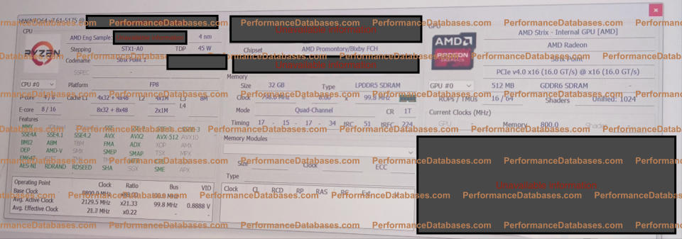
The 8,888 MHz base clock speed is obviously an error. The average active clock, which was 2,129.5 MHz, looks more reasonable. Remember that this is ES silicon, so the clock speeds are usually lower than the retail product. Phoenix has a maximum boost clock speed of up to 5.2 GHz, so it'll be intriguing to see how Zen 5 clocks compared to Zen 4. Another HWiNFO screenshot shows the Strix Point chip paired with 32GB of LPDDR5-6400 memory. For comparison, Phoenix embraces LPDDR5X-7500 out of the gate, but the Strix Point FP8 platform may just be using slower memory for testing purposes.
Strix Point taps into the RDNA 3.5 graphics engine. The leak reveals the processor with eight WGPs (Workgroup Processors). It's equal to 16 compute units or 1,024 stream processors. The memory on the ES silicon is clocked at 800 MHz. Phoenix has a maximum of 12 RDNA 3 compute units; therefore, Strix Point has 33% more GPU cores, not to mention the upgraded RDNA 3.5 GPU cores. Regarding clock speeds, Phoenix boasts frequencies up to 2,800 MHz. HWiNFO listed the Strix Point ES chip with 512MB of GDDR6 memory, a blatant error given that the iGPU gets its memory from the system.
Strix Point will launch in 2024 and power the next generation of gaming laptops. It's unlikely that the APUs can replace discrete graphics cards. However, the RDNA 3.5 engine should provide an acceptable level of performance for casual gamers. Meanwhile, the same combination of Zen 5 and RDNA 3.5 graphics will also be coming to the desktop AM5 socket through the Granite Ridge series. However, the iGPUs on Granite Ridge probably won't be helpful outside of basic display tasks.

